![]()
WE PROVIDE SOLUTIONS
- Home
- Products
- Double Layer
- Technical Capabilities
Technical Capabilities for Double Sided PCBs
| Capabilities | Minimum Capability | Maximum Capability | Tolerance | Remarks |
|---|---|---|---|---|
|
Metal finishing: |
|
|
Sn100C Alloyage |
|
|
Final finishing: |
|
- |
|
A wide range of colours A wide range of colours |
| Raw Material: FR-4 Tg Standard FR-4 High Tg |
130 ºC 150 ºC |
140 ºC 180 ºC |
-
|
Depending on the manufacturer |
|
Base Copper |
17 µm | 70 µm | - | Under request (consult delivery time): 105 µm |
|
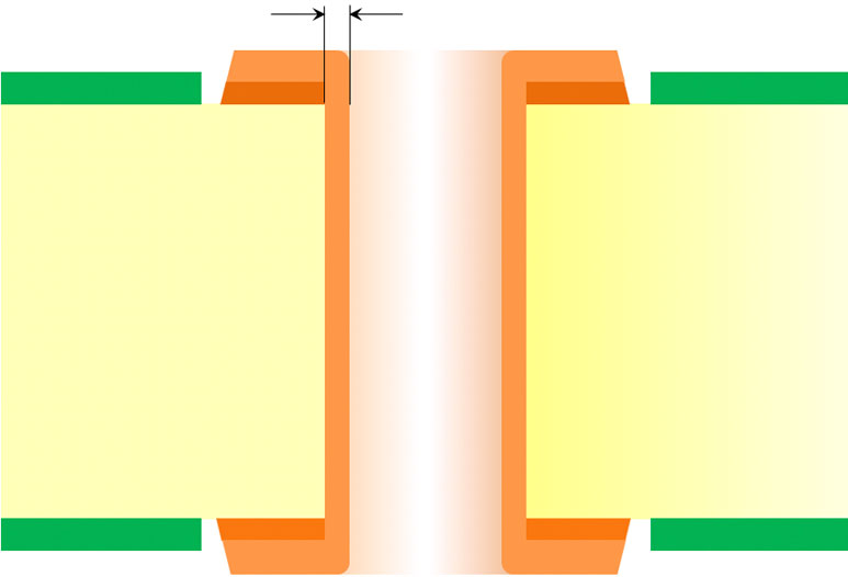
Platted Through Hole (PTH)
|
200 µm | - | + 0,10 / - 0,05 mm | Or equivalent tolerance |
|
Non Platted Through Hole (NPTH)
|
300 µm | - | + 0,10 / -0 mm | Or equivalent tolerance |
|
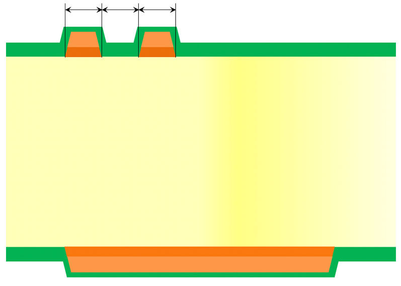
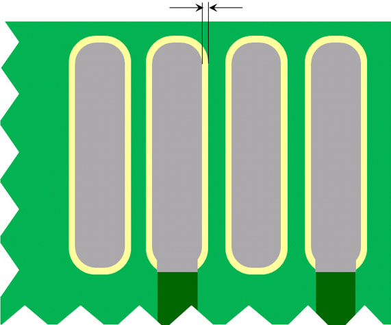
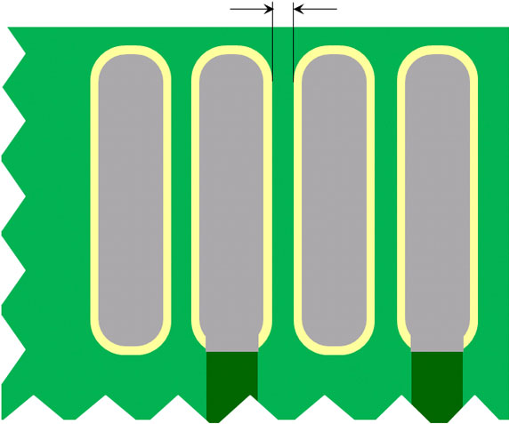
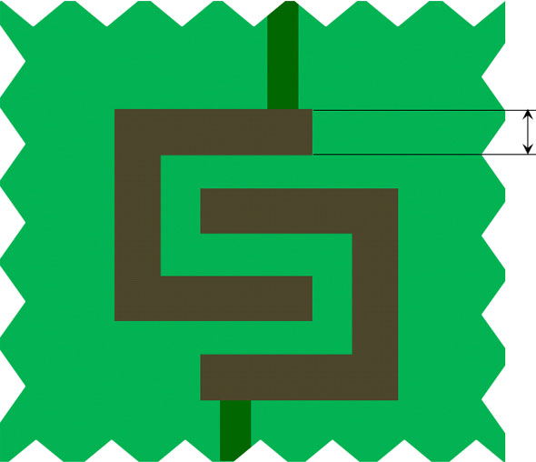
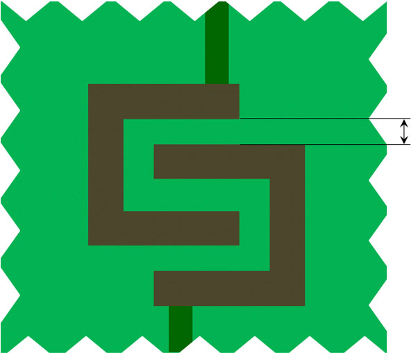
Width and isolation of copper conductors (Base Copper)
|
100 µm (17 µm) 125 µm (35 µm) 200 µm (70 µm) |
- | ± 25% ± 30% ± 30% |
- |
|
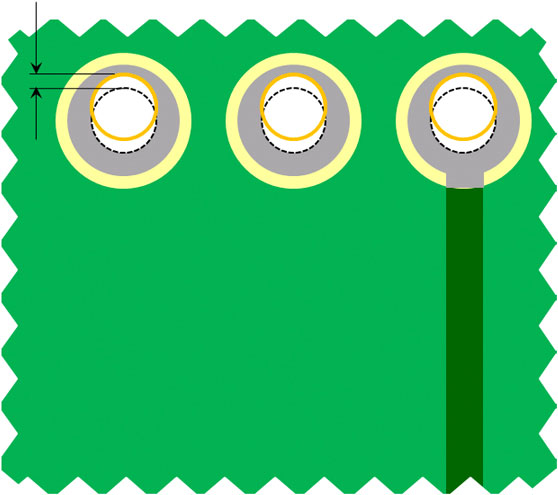
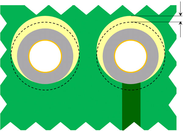
Copper annular ring (Base Copper)
|
100 µm (17 µm) |
- | - | Recommendation: for a good soldering surface, for component holes = 200 µm |
|
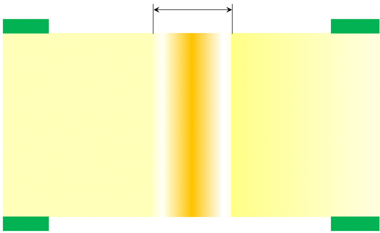
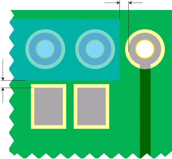
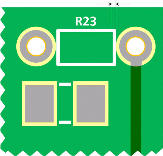
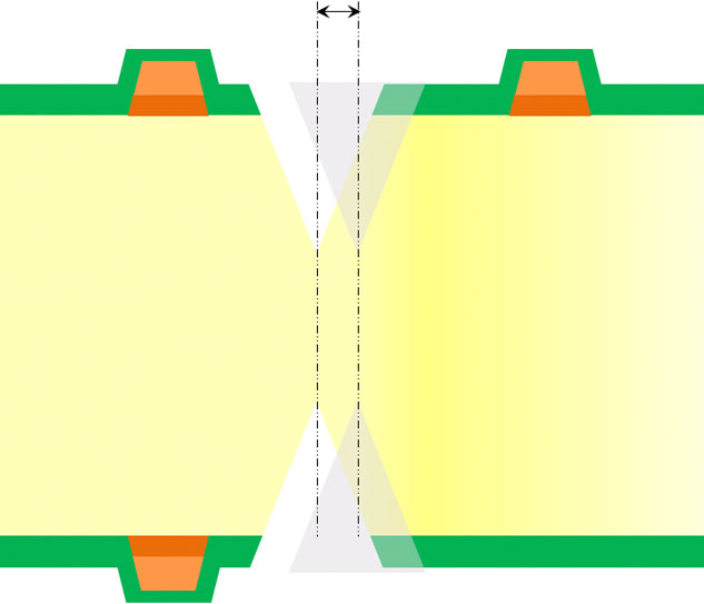
Distance between NPTH and copper conductor
|
200 µm | - | - | - |
|
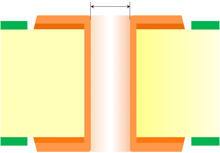
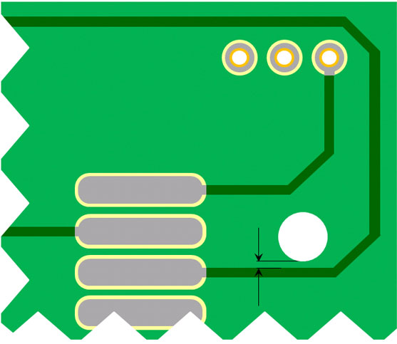
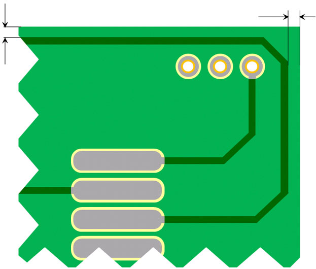
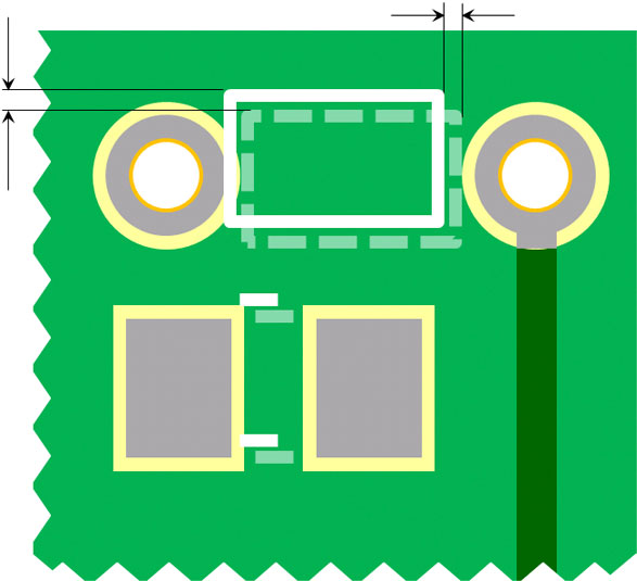
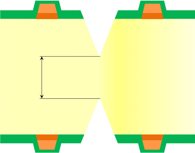
Distance between copper conductor and board edge (routed)
|
150 µm | - | - | - |
|
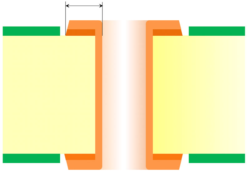
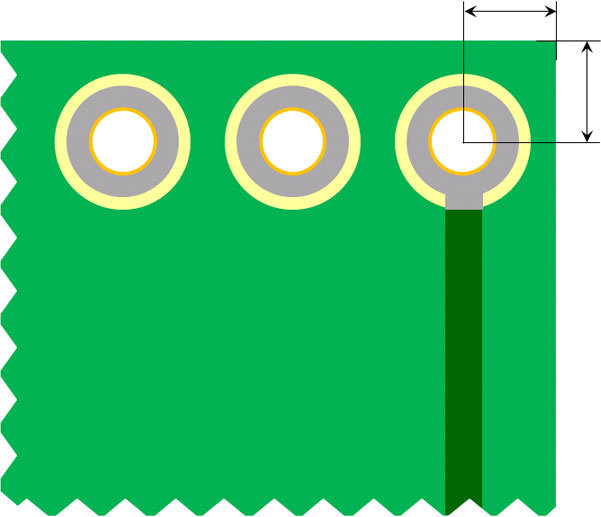
Misalignement between copper and PTH
|
- | - | ± 100 µm | - |
|
Misalignement between outline and PTH
|
- | ± 150 µm | ||
|
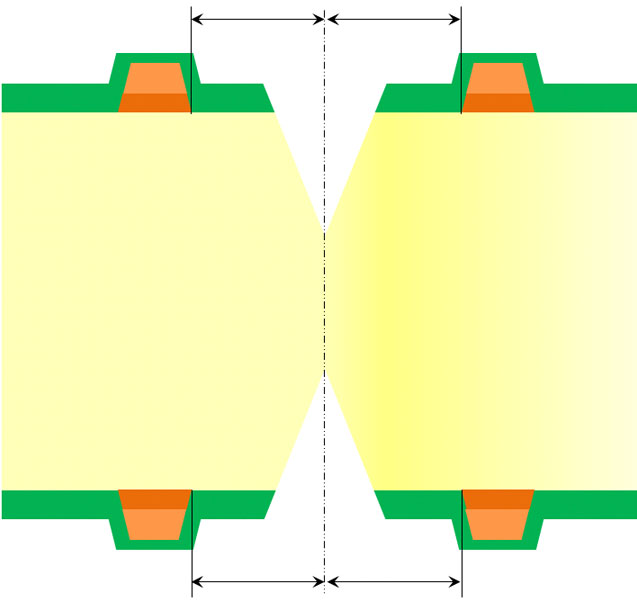
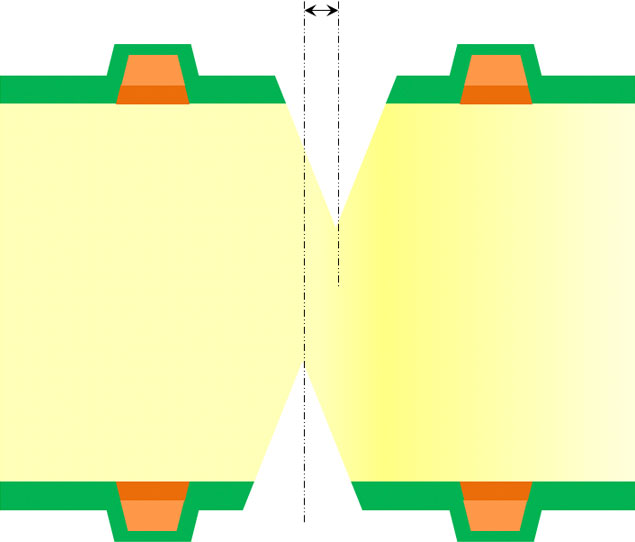
Distance between a copper conductor and theorical scoring axis
|
500 µm | - | - | - |
|
Maximum hole to be plugged with peelable mask
|
0,30 mm | 1,80 mm | - | - |
|
Distance between peelable mask and copper pad
|
0,80 mm | - | - | - |
|
Solder mask annular ring
|
50 µm | - | - | - |
|
Solder mask bridge
|
100 µm | - | - | - |
|
Distance between solder mask clearance and copper conductor
|
50 µm | - | - | - |
|
Misalignement between solder mask and copper
|
- | - | ± 150 µm | - |
|
Ink legend width
|
100 µm | - | - | - |
|
Misalignement between ink legend and copper
|
- | - | ± 200 µm | - |
|
Carbon Ink width
|
600 µm | - | - | - |
|
Separation between carbon conductors
|
400 µm | - | - | - |
|
Platted wall thickness
|
20 µm | 60 µm | - | Average: 25 µm |
|
Scoring positioning (taken on axis)
|
- | - | ± 150 µm | - |
|
Core thickness after scoring process
|
200 µm | - | ± 150 µm | Standard: 300 µm |
|
Misalignement between top-bottom scoring blades
|
- | - | ± 150 µm | - |
|
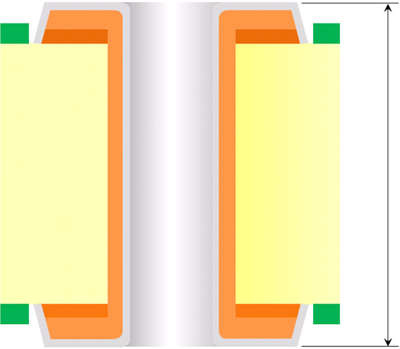
Final Thickness
|
0,50 mm | 3,2 mm |
± 10 % (e > 1,0 mm) |
- |
|
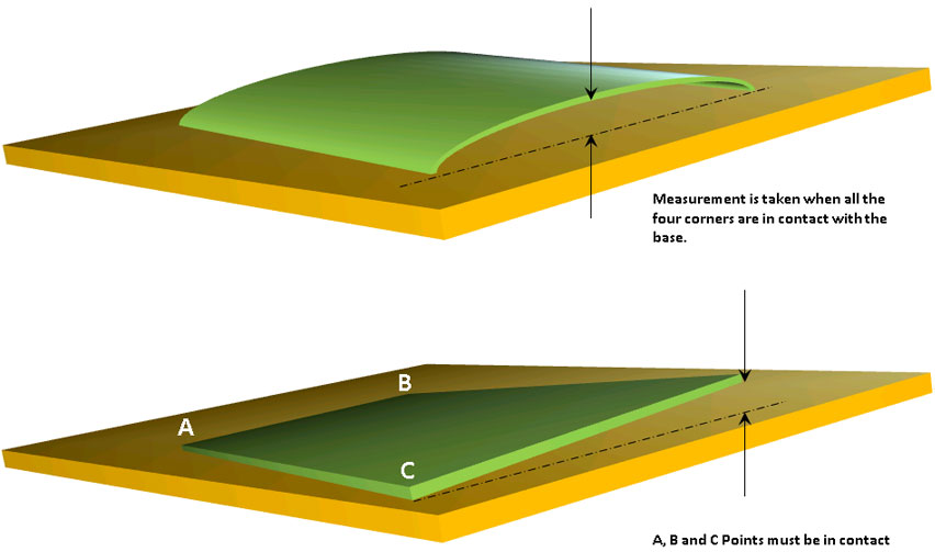
Bow&Twist
|
- | 0,75% of diagonal | - | - |
|
Final pcb dimensions (routing)
|
15 x 15 mm | 600 x 500 mm | < 30 mm: ± 0.10 mm < 120 mm: ± 0.15 mm >120 mm: ± 0.20 mm |
- |
|
Other |
- | - | - | According to IPC-A-600 revision G Standard |

REMARKS
The extra Cu deposition is performed by an electrolytic process; therefore It is extremely convenient that the density of Cu on both sides is similar. This reduces the irregularities in total Cu thickness, warping and bending, reduction in PTH diameters and the excess of Cu on conductors.
Need help?
Send us your contact details and one of our Sales agents will contact you as soon as possible.