![]()
WE PROVIDE SOLUTIONS
- Home
- Products
- Single Layer
- Technical Capabilities
Technical Capabilities for Single Sided Boards
| Capabilities | Minimum Capability | Maximum Capability | Tolerance | Remarks |
|---|---|---|---|---|
|
Metal finishing: |
|
|
- |
Not available for IMS pcbs |
|
Final finishing: |
- |
- |
- |
A wide range of colours A wide range of colours |
|
Raw Material: |
130 ºC |
140 ºC |
- |
Depending on the manufacturer |
|
Base Copper:
|
|
|
Under request (consult delivery time): 105 μm |
|
|
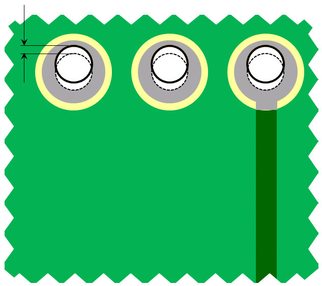
NTPH diameter (base material)
|
300 μm (FR-4 and CEM-1)
|
- | + 0,10 / -0 mm | Or equivalent tolerance |
|
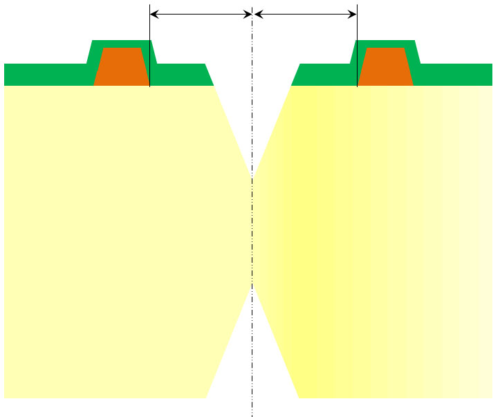
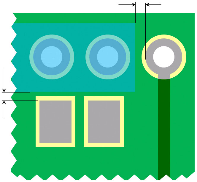
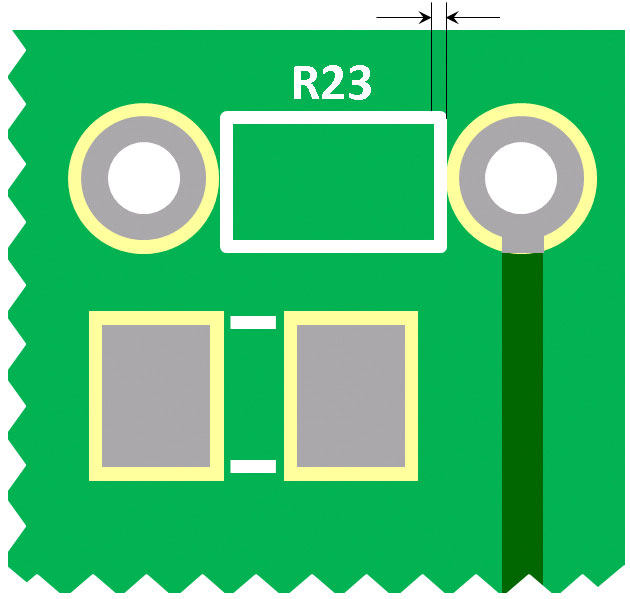
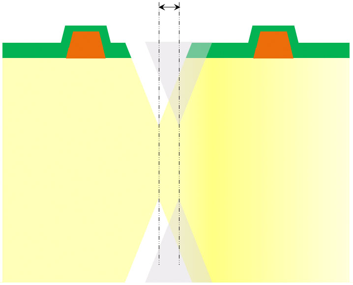
Width and isolation of copper conductors (Base Copper)
|
100 μm (17 μm) 200 µm (70 µm) |
- | ± 25% ± 25% ± 30% |
- |
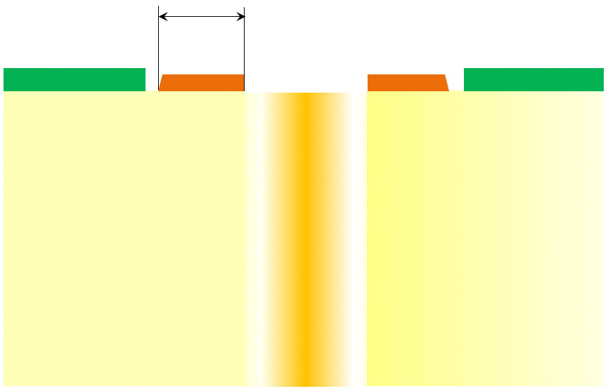
|
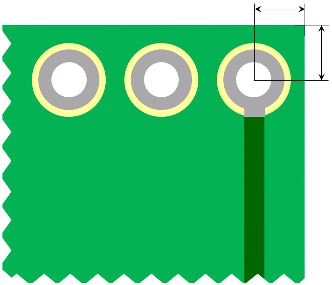
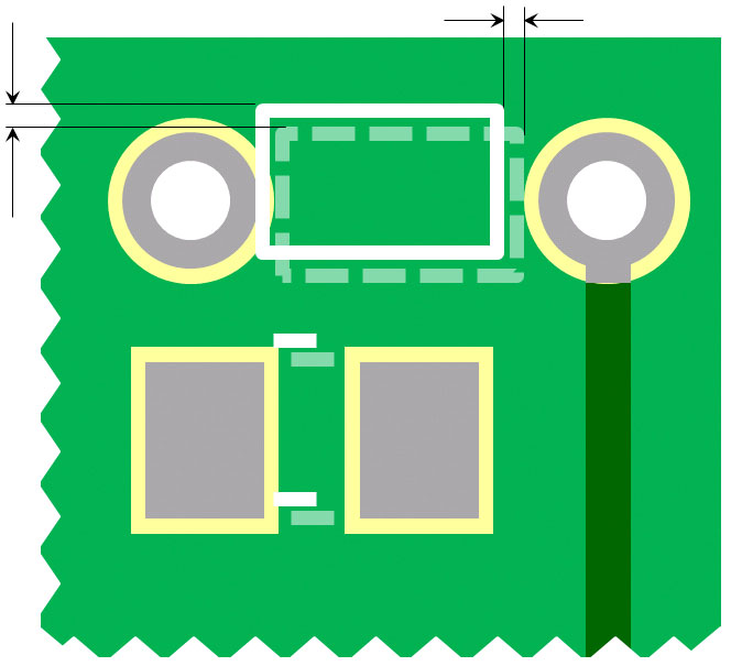
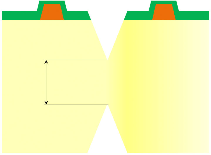
Copper annular ring (Base Copper)
|
100 μm (17 μm) |
- | Recommendation: for a good soldering surface, for component holes ≥ 200 µm | |
|
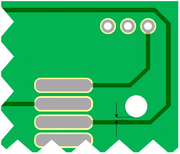
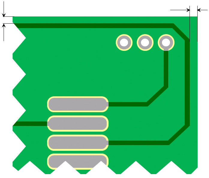
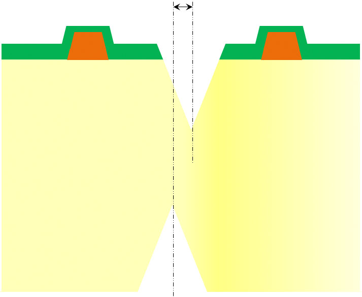
Distance between NPTH and copper conductor
|
200 µm | - | - | - |
|
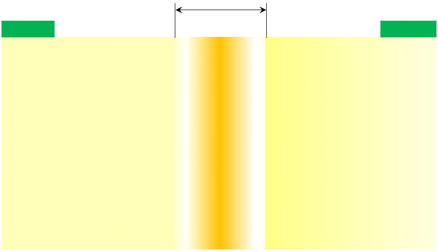
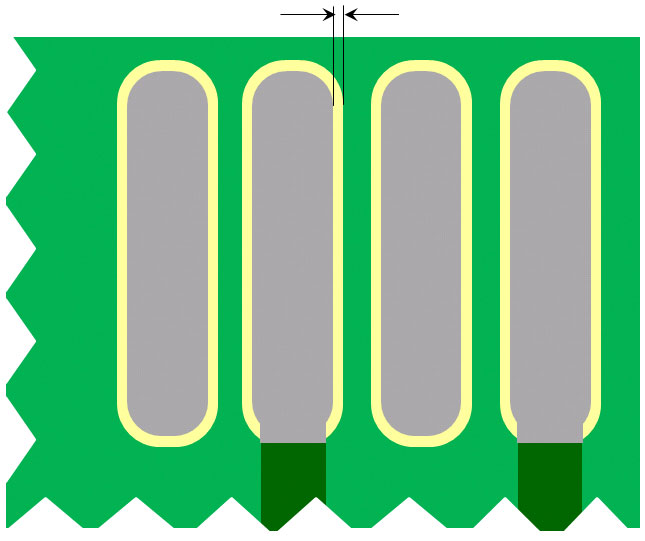
Distance between copper conductor and board edge (routed)
|
150 µm | - | - | - |
|
Misalignement between copper and hole
|
- | - | ± 100 µm | - |
|
Misalignement between outline and hole
|
- | ± 150 µm | ||
|
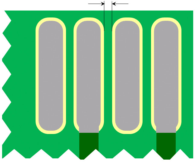
Distance between a copper conductor and theorical scoring axis
|
500 µm | - | - | - |
|
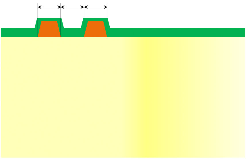
Maximum hole to be plugged with peelable mask
|
0,30 mm | 1,80 mm | - | - |
|
Distance between peelable mask and copper pad
|
0,80 mm | - | - | - |
|
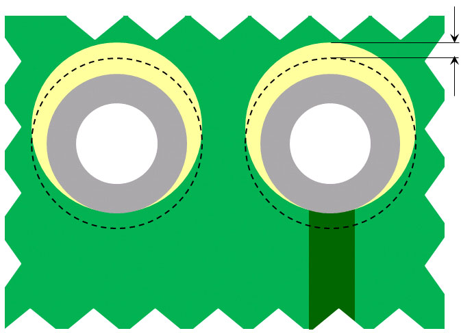
Solder mask annular ring
|
50 µm | - | - | - |
|
Solder mask bridge
|
100 µm | - | - | - |
|
Distance between solder mask clearnace and copper conductor
|
50 µm | - | - | - |
|
Misalignement between solder mask and copper
|
- | - | ± 150 µm | - |
|
Ink legend width
|
100 µm | - | - | - |
|
Misalignement between ink legend and copper
|
- | - | ± 200 µm | - |
|
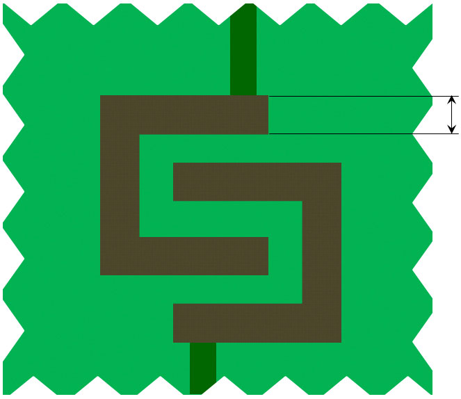
Carbon Ink width
|
600 µm | - | - | - |
|
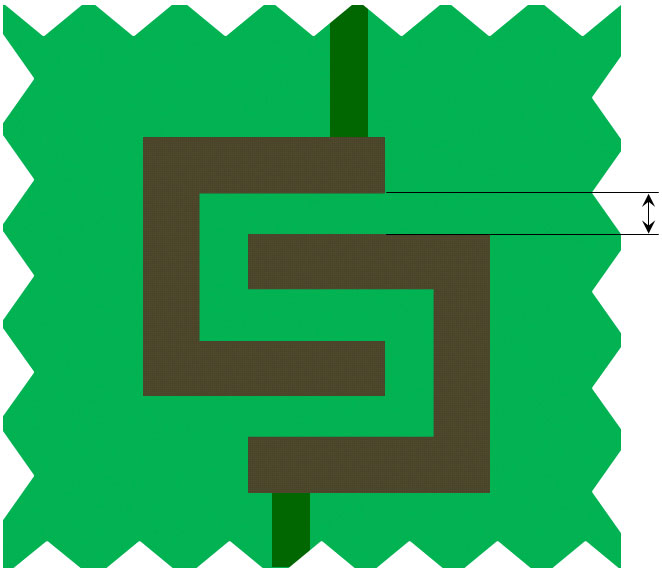
Separation between carbon conductors
|
400 µm | - | - | - |
|
Scoring positioning (taken on axis)
|
- | - | ± 150 µm | - |
|
Core thickness after scoring process
|
200 µm | - | ± 150 µm | Standard: 300 µm |
|
Misalignement between top-bottom scoring blades
|
- | - | ± 150 µm | - |
|
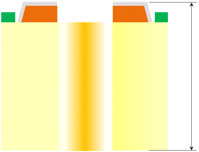
Final Thickness
|
0,50 mm 1,0 mm 1,0 mm |
3,2 mm 1,6 mm 3,0 mm |
± 10 % (e > 1,0 mm) and ± 100 μm (e ≤ 1,0 mm) ± 10 % ± 10 % |
For FR-4 raw material For CEM-1 raw material For IMS raw material |
|
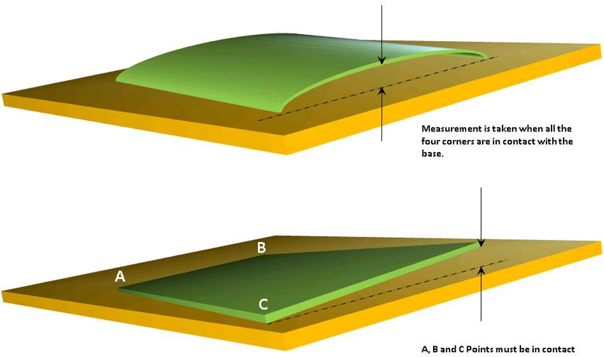
Bow&Twist
|
- | 1% of diagonal | - | - |
|
Final pcb dimensions (routing)
|
15 x 15 mm | 600 x 500 mm | < 30 mm: ± 0.10 mm < 120 mm: ± 0.15 mm >120 mm: ± 0.20 mm |
- |
| Other | - | - | - | According to IPC-A-600 revision G Standard |


Need help?
Send us your contact details and one of our Sales agents will contact you as soon as possible.